Single-layer PCBs consist of a single conductive layer, making them simpler and more cost-effective for basic electronic circuits with limited components. Multi-layer PCBs feature multiple conductive layers separated by insulating materials, enabling higher circuit density, enhanced signal integrity, and improved electromagnetic interference (EMI) reduction. Choosing between single-layer and multi-layer PCBs depends on the complexity, size, and electrical performance requirements of the hardware design.
Table of Comparison
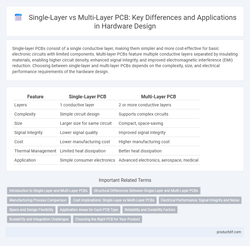
| Feature | Single-Layer PCB | Multi-Layer PCB |
|---|---|---|
| Layers | 1 conductive layer | 2 or more conductive layers |
| Complexity | Simple circuit design | Supports complex circuits |
| Size | Larger size for same circuit | Compact, space-saving |
| Signal Integrity | Lower signal quality | Improved signal integrity |
| Cost | Lower manufacturing cost | Higher manufacturing cost |
| Thermal Management | Limited heat dissipation | Better heat dissipation |
| Application | Simple consumer electronics | Advanced electronics, aerospace, medical |
Introduction to Single-Layer and Multi-Layer PCBs
Single-layer PCBs consist of a single conductive layer on one side of an insulating substrate, ideal for simple, low-cost electronic devices with minimal circuitry requirements. Multi-layer PCBs contain multiple conductive layers separated by insulating materials, enabling compact and complex circuit designs with improved signal integrity and reduced electromagnetic interference. The choice between single-layer and multi-layer PCBs depends on factors such as design complexity, space constraints, and electrical performance needs.
Structural Differences Between Single-Layer and Multi-Layer PCBs
Single-layer PCBs consist of a single conductive copper layer laminated onto a non-conductive substrate, typically fiberglass, offering a simple structure with limited routing options. Multi-layer PCBs comprise multiple copper layers separated by insulating dielectric materials, enabling complex circuit designs and higher component density. The structural complexity of multi-layer PCBs allows for enhanced electrical performance, signal integrity, and the integration of advanced features such as embedded components and controlled impedance.
Manufacturing Process Comparison
Single-layer PCBs feature a straightforward manufacturing process involving a single copper layer bonded to the substrate, allowing for simpler etching and drilling steps, which reduces production time and cost. Multi-layer PCBs require complex lamination procedures with multiple insulating layers and copper foils, necessitating precise alignment and advanced via drilling techniques that increase manufacturing complexity and cost. The intricate fabrication of multi-layer PCBs results in enhanced circuit density and reliability but demands high-tech equipment and stringent quality control during production.
Cost Implications: Single-Layer vs Multi-Layer PCBs
Single-layer PCBs offer a lower manufacturing cost due to simpler design and fewer materials, making them ideal for basic electronic devices and low-volume production. Multi-layer PCBs incur higher costs driven by complex fabrication processes, increased raw materials, and advanced drilling techniques required to stack multiple insulating and conductive layers. Cost implications also impact overall project budgets, where multi-layer PCBs justify the expense through enhanced performance, reduced size, and higher component density for sophisticated applications.
Electrical Performance: Signal Integrity and Noise
Single-layer PCBs often struggle with signal integrity due to limited routing options and increased electromagnetic interference, making them less ideal for high-frequency applications. Multi-layer PCBs enhance electrical performance by providing dedicated ground and power planes that reduce noise and improve signal return paths, minimizing crosstalk and electromagnetic interference. These design improvements in multi-layer PCBs ensure superior signal integrity and reliability in complex, high-speed circuits.
Space and Design Flexibility
Single-layer PCBs offer simplicity and cost-effectiveness but are limited in space and design flexibility due to having only one conductive layer, which restricts circuit complexity and component density. Multi-layer PCBs provide enhanced space utilization by stacking multiple conductive layers separated by insulating materials, enabling compact designs and complex routing paths suitable for advanced electronic devices. This layered architecture significantly increases design flexibility, allowing for higher component density and improved electrical performance in compact hardware systems.
Application Areas for Each PCB Type
Single-layer PCBs are ideal for simple electronic devices such as calculators, power supplies, and LED lighting due to their cost-effectiveness and straightforward design. Multi-layer PCBs support complex applications like computer motherboards, medical equipment, and telecommunications hardware, where high-density circuitry and enhanced performance are critical. The choice between single-layer and multi-layer PCBs depends heavily on the device's complexity, signal integrity requirements, and space constraints.
Reliability and Durability Factors
Single-layer PCBs offer simplicity and ease of manufacturing but are more prone to signal interference and physical damage due to their single conductive layer, impacting long-term reliability. Multi-layer PCBs enhance durability and performance by incorporating multiple layers of insulation and conductive pathways, reducing electromagnetic interference and improving heat dissipation. These structural advantages make multi-layer PCBs more suitable for complex, high-density applications requiring superior reliability and extended operational lifespan.
Scalability and Integration Challenges
Single-layer PCBs offer limited scalability due to their single conductive layer, restricting complex circuit design and integration capabilities. Multi-layer PCBs enable higher component density and enhanced signal integrity by stacking multiple layers, supporting complex, scalable hardware systems. Integration challenges in multi-layer PCBs include precise layer alignment and managing inter-layer insulation to ensure reliable electrical performance.
Choosing the Right PCB for Your Product
Selecting the right PCB depends on product complexity, signal integrity, and space constraints. Single-layer PCBs offer cost-effective solutions for simple circuits with minimal interference, while multi-layer PCBs provide enhanced performance through additional conductive layers, enabling higher component density and improved electromagnetic compatibility. Understanding application requirements and budget helps determine whether a single-layer or multi-layer PCB best supports your product's functionality and reliability.
Single-Layer PCB vs Multi-Layer PCB Infographic