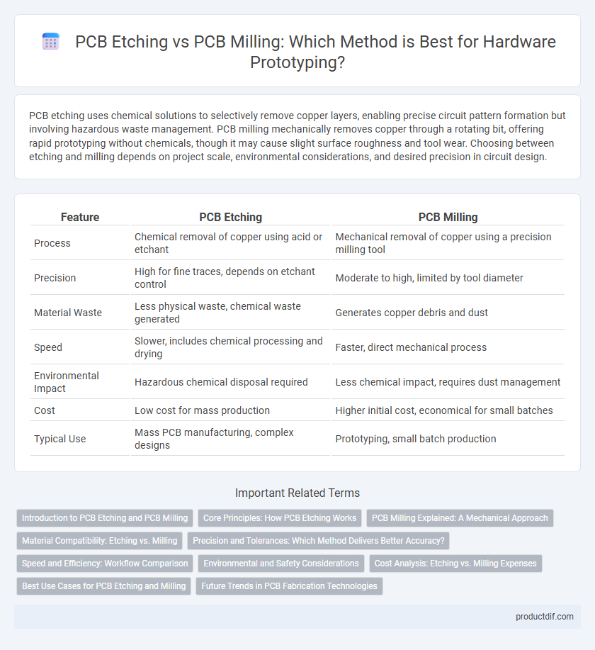
PCB etching uses chemical solutions to selectively remove copper layers, enabling precise circuit pattern formation but involving hazardous waste management. PCB milling mechanically removes copper through a rotating bit, offering rapid prototyping without chemicals, though it may cause slight surface roughness and tool wear. Choosing between etching and milling depends on project scale, environmental considerations, and desired precision in circuit design.
Table of Comparison
| Feature | PCB Etching | PCB Milling |
|---|---|---|
| Process | Chemical removal of copper using acid or etchant | Mechanical removal of copper using a precision milling tool |
| Precision | High for fine traces, depends on etchant control | Moderate to high, limited by tool diameter |
| Material Waste | Less physical waste, chemical waste generated | Generates copper debris and dust |
| Speed | Slower, includes chemical processing and drying | Faster, direct mechanical process |
| Environmental Impact | Hazardous chemical disposal required | Less chemical impact, requires dust management |
| Cost | Low cost for mass production | Higher initial cost, economical for small batches |
| Typical Use | Mass PCB manufacturing, complex designs | Prototyping, small batch production |
Introduction to PCB Etching and PCB Milling
PCB etching involves chemically removing unwanted copper from a laminated board to create precise circuit patterns, making it ideal for complex and high-density designs. PCB milling uses a mechanical process where a CNC machine physically carves out the copper layer, offering faster prototyping and chemical-free fabrication. Both techniques demand careful consideration of board material, design complexity, and production volume to select the most efficient manufacturing method.
Core Principles: How PCB Etching Works
PCB etching involves selectively removing copper from a laminated board using chemical solutions like ferric chloride, creating precise circuit patterns based on a photoresist mask. The process begins by applying a photosensitive layer that hardens when exposed to UV light, protecting desired copper sections while exposing unwanted areas to the etchant. This controlled chemical reaction ensures high-resolution traces and consistent layer thickness, essential for reliable PCB performance and complex multilayer designs.
PCB Milling Explained: A Mechanical Approach
PCB milling employs precision mechanical tools to remove copper layers from a substrate, creating the circuit pattern without the need for chemicals. This method offers high accuracy for prototype and small-scale production runs, reducing environmental impact compared to traditional etching processes. Milling machines utilize CNC technology to achieve fine detail and consistent trace widths, making it ideal for complex multi-layer boards.
Material Compatibility: Etching vs. Milling
PCB etching thrives on compatibility with copper-clad laminate materials such as FR-4 and CEM-1, effectively dissolving unwanted copper layers with chemical solutions like ferric chloride or ammonium persulfate. PCB milling excels in versatility, accommodating diverse substrates including aluminum, ceramic, and flexible materials by mechanically removing copper without chemical exposure. Material compatibility directly impacts the choice between etching and milling processes, influencing factors like resolution, environmental considerations, and substrate integrity.
Precision and Tolerances: Which Method Delivers Better Accuracy?
PCB milling offers higher precision and tighter tolerances than PCB etching due to its mechanical removal of copper with CNC-controlled tools, enabling micron-level accuracy. Etching relies on chemical processes that can cause undercutting and uneven copper removal, leading to less consistent trace widths and spacing. For applications requiring fine detail and stringent dimensional control, PCB milling is the preferred method for delivering superior accuracy.
Speed and Efficiency: Workflow Comparison
PCB etching offers faster batch processing for high-volume production due to its chemical-based removal of copper layers, while PCB milling provides quicker prototyping capabilities with precise mechanical cutting. Milling enables immediate adjustments and less setup time, ideal for iterative design workflows, whereas etching requires longer preparation and safety protocols impacting overall efficiency. Choosing between etching and milling depends on balancing throughput speed with flexibility in the manufacturing process.
Environmental and Safety Considerations
PCB etching uses chemical solutions like ferric chloride or ammonium persulfate, which require careful disposal to prevent environmental contamination and pose health risks due to toxic fumes. PCB milling eliminates chemical use by mechanically removing copper, reducing hazardous waste and improving operator safety but generates particulate debris needing proper collection. Both processes mandate strict safety protocols, but milling offers a more environmentally friendly alternative by minimizing chemical pollutants.
Cost Analysis: Etching vs. Milling Expenses
PCB etching typically incurs lower initial equipment costs compared to milling machines, making it more affordable for small-scale production. However, milling reduces chemical waste and the need for hazardous materials disposal, potentially lowering environmental compliance expenses over time. Overall, while etching offers cost advantages in materials, milling's precision and waste reduction can result in favorable long-term financial benefits depending on production volume.
Best Use Cases for PCB Etching and Milling
PCB etching is best suited for mass production of complex, multi-layered circuit boards with fine, precise traces due to its chemical-based process that allows high resolution and consistency. PCB milling excels in rapid prototyping and small batch runs where quick turnaround and easy modification are crucial, as it physically removes material using CNC machines without the need for hazardous chemicals. Etching provides superior surface finish and finer detail, while milling offers flexibility and minimal setup for iterative design testing.
Future Trends in PCB Fabrication Technologies
Future trends in PCB fabrication emphasize advanced etching techniques using environmentally friendly chemicals and precision laser etching to achieve finer circuit details. PCB milling is evolving with high-speed, multi-axis CNC machines that improve accuracy and reduce material waste for rapid prototyping. Integration of AI-driven process optimization and in-situ monitoring systems aims to enhance yield and consistency in both etching and milling methods.
PCB etching vs PCB milling Infographic