Single-layer PCBs consist of a single conductive layer, making them simpler and more cost-effective for basic hardware pet designs with fewer components. Multilayer PCBs feature multiple stacked layers, allowing for higher circuit density, improved signal integrity, and enhanced overall performance in complex hardware pet applications. Choosing between single-layer and multilayer PCBs depends on the complexity, size constraints, and electrical requirements of the hardware pet project.
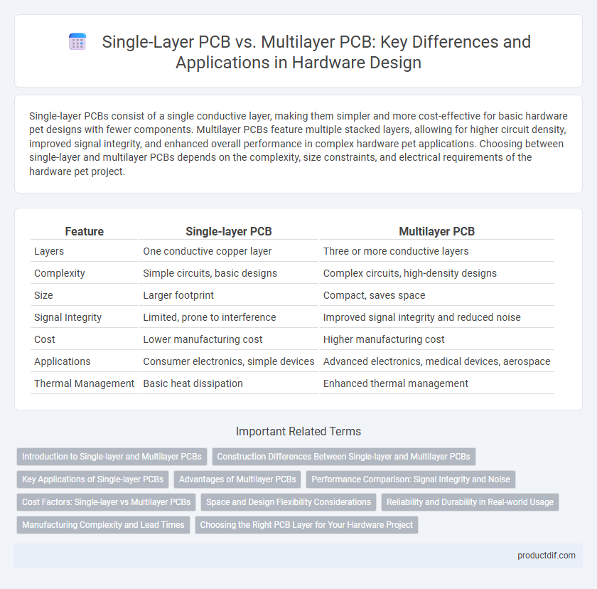
Table of Comparison
| Feature | Single-layer PCB | Multilayer PCB |
|---|---|---|
| Layers | One conductive copper layer | Three or more conductive layers |
| Complexity | Simple circuits, basic designs | Complex circuits, high-density designs |
| Size | Larger footprint | Compact, saves space |
| Signal Integrity | Limited, prone to interference | Improved signal integrity and reduced noise |
| Cost | Lower manufacturing cost | Higher manufacturing cost |
| Applications | Consumer electronics, simple devices | Advanced electronics, medical devices, aerospace |
| Thermal Management | Basic heat dissipation | Enhanced thermal management |
Introduction to Single-layer and Multilayer PCBs
Single-layer PCBs consist of a single insulating substrate with a single conductive copper layer used to connect electronic components, making them suitable for simple, low-cost applications. Multilayer PCBs feature multiple insulating layers separated by conductive copper layers, allowing complex circuits with higher component density and improved electrical performance. The choice between single-layer and multilayer PCBs depends on factors like circuit complexity, signal integrity requirements, and overall device design constraints.
Construction Differences Between Single-layer and Multilayer PCBs
Single-layer PCBs consist of a single conductive layer of copper on one side of the substrate, making them simpler in construction and ideal for low-density designs. Multilayer PCBs contain multiple copper layers separated by insulating layers, allowing for complex circuit routing and higher component density within a compact footprint. The construction differences directly impact electrical performance, signal integrity, and overall durability of the final hardware product.
Key Applications of Single-layer PCBs
Single-layer PCBs are widely utilized in consumer electronics such as radios, calculators, and printers due to their simple design and cost-effectiveness. These PCBs are ideal for applications requiring low circuit density and minimal complexity, including power supplies and LED lighting systems. Their ease of manufacturing and repair makes them suitable for prototyping and low-volume production runs in the hardware industry.
Advantages of Multilayer PCBs
Multilayer PCBs offer superior electrical performance by reducing signal interference and enabling higher circuit density compared to single-layer PCBs. Their compact design allows for efficient use of space in complex electronic devices like smartphones, medical instruments, and aerospace equipment. Enhanced durability and improved thermal management further provide reliability in high-frequency and high-power applications.
Performance Comparison: Signal Integrity and Noise
Multilayer PCBs offer superior signal integrity compared to single-layer PCBs due to dedicated ground and power planes that reduce electromagnetic interference and crosstalk. Single-layer PCBs are more prone to noise and signal degradation because of their limited routing capability and lack of internal shielding layers. High-frequency applications benefit significantly from multilayer PCB designs, ensuring stable signal transmission and reduced noise susceptibility.
Cost Factors: Single-layer vs Multilayer PCBs
Single-layer PCBs are generally more cost-effective due to simpler manufacturing processes, lower material usage, and reduced design complexity. Multilayer PCBs incur higher costs driven by increased material consumption, more complex fabrication steps, and additional testing requirements. The price difference significantly impacts product budgeting, especially in high-volume electronics manufacturing.
Space and Design Flexibility Considerations
Single-layer PCBs offer limited space and design flexibility due to their single conductive layer, making them suitable for simple circuits with fewer components. Multilayer PCBs maximize available space by stacking multiple conductive layers, enabling complex designs and higher component density within compact footprints. This multilayer structure enhances signal integrity and allows for advanced routing options in sophisticated hardware applications.
Reliability and Durability in Real-world Usage
Single-layer PCBs offer simplicity and lower cost but typically lack the durability and reliability required for complex or high-stress applications. Multilayer PCBs enhance reliability by providing better electrical performance with shorter interconnections and improved signal integrity, making them more resilient to environmental factors such as vibration and thermal stress. In real-world usage, multilayer PCBs demonstrate superior durability and longevity, especially in automotive, aerospace, and high-frequency electronic devices where reliability is critical.
Manufacturing Complexity and Lead Times
Single-layer PCBs feature a straightforward manufacturing process with fewer steps, resulting in shorter lead times and lower production costs. Multilayer PCBs require advanced fabrication techniques including precise layer alignment and lamination, increasing manufacturing complexity and extending lead times significantly. The added complexity in multilayer PCB production demands specialized equipment and stringent quality controls to ensure reliability and performance.
Choosing the Right PCB Layer for Your Hardware Project
Choosing the right PCB layer depends on your hardware project's complexity and electrical requirements; single-layer PCBs are ideal for simple circuits with minimal components, offering cost-effectiveness and ease of manufacturing. Multilayer PCBs support higher density designs, improved signal integrity, and reduced electromagnetic interference, making them suitable for advanced applications like aerospace, medical devices, and high-speed computing. Evaluate factors such as space constraints, signal routing complexity, and budget to determine whether a single-layer or multilayer PCB best meets your project's performance and reliability needs.
Single-layer PCB vs Multilayer PCB Infographic