PCB layout defines the placement of components on the board, optimizing space and ensuring electrical performance. PCB routing establishes the electrical connections between these components through copper traces, impacting signal integrity and impedance. Effective coordination of layout and routing is crucial for minimizing noise, reducing interference, and enhancing overall circuit reliability.
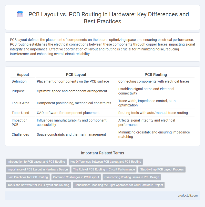
Table of Comparison
| Aspect | PCB Layout | PCB Routing |
|---|---|---|
| Definition | Placement of components on the PCB surface | Connecting components with electrical traces |
| Purpose | Optimize space and component arrangement | Establish signal paths and electrical connectivity |
| Focus Area | Component positioning, mechanical constraints | Trace width, impedance control, path optimization |
| Tools Used | CAD software for component placement | Routing tools with auto/manual trace routing |
| Impact on PCB | Influences manufacturability and component accessibility | Affects signal integrity and electrical performance |
| Challenges | Space constraints and thermal management | Minimizing crosstalk and ensuring impedance matching |
Introduction to PCB Layout and PCB Routing
PCB layout involves designing the physical arrangement of components and their connections on the circuit board, ensuring optimal space utilization and signal integrity. PCB routing focuses on creating the electrical paths that connect components, taking into account factors like impedance, trace width, and layer stacking to minimize noise and interference. Both processes are critical for functional, reliable printed circuit boards in hardware design.
Key Differences Between PCB Layout and PCB Routing
PCB layout involves the strategic placement of electronic components on the board, prioritizing space efficiency and signal integrity. PCB routing focuses on creating electrical connections between components by designing conductive pathways that minimize noise and impedance issues. Key differences include layout's emphasis on component arrangement and mechanical constraints, while routing centers on optimizing trace paths for performance and manufacturability.
Importance of PCB Layout in Hardware Design
PCB layout plays a critical role in hardware design by defining the precise placement of components and ensuring optimal signal integrity across the board. Proper PCB layout minimizes electromagnetic interference (EMI), reduces crosstalk, and enhances thermal management, which are essential for reliable device performance. Effective layout decisions directly impact the efficiency of subsequent PCB routing, ultimately influencing the functionality and manufacturability of electronic hardware.
The Role of PCB Routing in Circuit Performance
PCB routing directly influences circuit performance by determining signal integrity, electromagnetic compatibility, and power distribution efficiency. Optimal routing minimizes crosstalk, reduces noise, and controls impedance, which are critical for high-speed and RF circuits. Effective PCB routing strategies enhance overall device reliability and operational stability by ensuring precise electrical connections and reducing parasitic effects.
Step-by-Step PCB Layout Process
PCB layout involves the strategic placement of components on a printed circuit board, ensuring optimal space utilization and signal integrity before routing traces. The step-by-step PCB layout process begins with schematic capture, followed by defining board outlines, placing components according to design rules, and performing design rule checks (DRC) to prevent layout errors. Effective layout is crucial for minimizing trace lengths and electromagnetic interference, setting the foundation for efficient PCB routing that connects components with precise electrical paths.
Best Practices for PCB Routing
Effective PCB routing demands minimizing trace lengths and avoiding sharp angles to reduce signal interference and maintain signal integrity. Maintaining consistent trace widths and spacing adheres to impedance requirements and prevents crosstalk, which is critical for high-speed circuit designs. Employing multi-layer boards and proper via placement enhances routing efficiency while ensuring optimal electrical performance and thermal management.
Common Challenges in PCB Layout
Common challenges in PCB layout include managing component placement to minimize signal interference and ensure efficient power distribution, which directly impacts overall circuit performance. Designers must optimize trace routing paths while balancing electrical constraints such as impedance control, crosstalk reduction, and thermal management. Addressing these challenges requires advanced software tools and a deep understanding of electromagnetic compatibility (EMC) principles to prevent signal degradation and mechanical failures.
Overcoming Routing Issues in PCB Design
Effective PCB layout ensures optimal component placement to minimize complexity during PCB routing, directly impacting signal integrity and manufacturability. Overcoming routing issues involves careful consideration of trace width, spacing, and layer stack-up to prevent crosstalk, impedance mismatches, and thermal problems. Utilizing Design for Manufacturability (DFM) guidelines and advanced routing algorithms enhances the overall reliability and performance of complex PCB designs.
Tools and Software for PCB Layout and Routing
PCB layout tools focus on component placement and layer stack visualization, optimizing space and signal integrity in software like Altium Designer and KiCad. PCB routing software, integrated within these platforms or as dedicated tools such as Cadence Allegro, automates trace path creation while minimizing crosstalk and interference. Advanced solutions leverage features like autorouters, design rule checks (DRCs), and real-time 3D modeling to enhance both the layout and routing phases of PCB design.
Conclusion: Choosing the Right Approach for Your Hardware Project
Selecting the right approach between PCB layout and PCB routing is crucial for optimizing hardware performance and reliability. PCB layout focuses on component placement and overall board design, while PCB routing emphasizes electrical connectivity and signal integrity. Prioritizing a balanced integration of both ensures efficient manufacturing, reduced signal interference, and enhanced device functionality.
PCB Layout vs PCB Routing Infographic