JTAG debugging offers a standardized 4- or 5-pin interface designed for testing and programming complex integrated circuits, providing broad compatibility with various microcontrollers. SWD (Serial Wire Debug) debugging uses a simplified 2-pin interface, optimizing pin usage while maintaining efficient debugging and programming capabilities, especially suited for ARM Cortex-M devices. Both protocols support breakpoint setting, memory access, and real-time debugging, but SWD's reduced pin count makes it ideal for resource-constrained embedded systems.
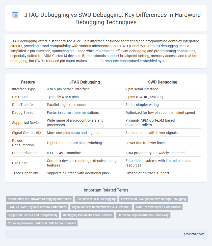
Table of Comparison
| Feature | JTAG Debugging | SWD Debugging |
|---|---|---|
| Interface Type | 4 to 5 pin parallel interface | 2 pin serial interface |
| Pin Count | Typically 4 or 5 pins | 2 pins (SWDIO, SWCLK) |
| Data Transfer | Parallel, higher pin count | Serial, simpler wiring |
| Debug Speed | Faster in some implementations | Optimized for low pin count, efficient speed |
| Supported Devices | Wide range of microcontrollers and processors | Primarily ARM Cortex-M based microcontrollers |
| Signal Complexity | More complex setup and signals | Simpler setup with fewer signals |
| Power Consumption | Higher due to more pins switching | Lower due to fewer lines |
| Standardization | IEEE 1149.1 standard | ARM proprietary but widely accepted |
| Use Case | Complex devices requiring extensive debug features | Embedded systems with limited pins and resources |
| Trace Capability | Supports full trace with additional pins | Limited or no trace support |
Introduction to Hardware Debugging Interfaces
JTAG debugging and SWD debugging are essential hardware debugging interfaces used to test and program microcontrollers. JTAG (Joint Test Action Group) interface supports complex boundary-scan testing and multi-core debugging, while SWD (Serial Wire Debug) provides a streamlined, two-pin communication protocol optimized for ARM microcontrollers. Selecting between JTAG and SWD depends on the specific device architecture, debugging requirements, and available hardware resources.
Overview of JTAG Debugging
JTAG debugging utilizes the IEEE 1149.1 standard to provide a boundary-scan interface for testing and programming microcontrollers and processors. It enables direct access to internal registers and memory through a dedicated multi-pin interface, facilitating complex debugging and device programming. JTAG supports a wide range of devices and is often preferred for comprehensive system-level diagnostics and development.
Overview of SWD (Serial Wire Debug) Debugging
Serial Wire Debug (SWD) is a two-pin interface designed for efficient debugging and programming of ARM Cortex-M microcontrollers, providing a compact alternative to the traditional JTAG interface. SWD uses a single data line and a clock line for bidirectional data transfer, enabling reduced pin usage while maintaining robust debug capabilities such as breakpoint setting, memory access, and real-time control. This streamlined interface enhances hardware design flexibility and is widely supported by modern development tools in embedded systems.
JTAG vs SWD: Key Architectural Differences
JTAG debugging uses a 4- or 5-pin interface that supports multiple devices on a single chain, enabling boundary-scan testing and complex system debug access. SWD debugging employs a 2-pin interface optimized for ARM Cortex processors, providing faster communication and reduced pin count with dedicated data (SWDIO) and clock (SWCLK) lines. The architectural difference centers on JTAG's broad compatibility with various chip designs versus SWD's streamlined protocol specifically tailored for ARM microcontrollers.
Signal and Pin Requirements: JTAG vs SWD
JTAG debugging requires multiple pins including TCK, TMS, TDI, TDO, and sometimes TRST, making it more pin-intensive compared to SWD. SWD debugging uses only two main signals, SWDIO and SWCLK, significantly reducing pin count and simplifying board layout. This streamlined pin requirement in SWD makes it ideal for resource-constrained embedded systems where minimizing I/O usage is critical.
Data Transfer Speed Comparison
JTAG debugging typically offers slower data transfer speeds, ranging from 1 to 10 Mbps, due to its multi-wire interface and complex signaling. In contrast, SWD debugging provides faster data transfer rates, often exceeding 10 Mbps, by using a streamlined two-wire protocol optimized for ARM-based microcontrollers. The increased efficiency of SWD makes it preferable for high-speed data acquisition and real-time debugging scenarios.
Supported Devices and Compatibility
JTAG debugging supports a wide range of devices across various architectures including ARM, MIPS, and x86, making it highly compatible with complex multi-core processors and legacy systems. SWD debugging, primarily designed for ARM Cortex-M microcontrollers, offers a streamlined two-pin interface that enhances compatibility with resource-constrained embedded devices. While JTAG provides broad device support ideal for advanced debugging scenarios, SWD's specialized compatibility ensures efficient communication with modern low-pin-count ARM devices.
Debugging Capabilities and Features
JTAG debugging supports complex boundary-scan testing and allows access to multiple devices on a single chain, providing comprehensive control over the entire system. SWD debugging uses a two-wire interface that simplifies communication and speeds up the debugging process, ideal for ARM Cortex microcontrollers with low pin count. Both methods enable breakpoint setting, memory inspection, and real-time data tracing, but JTAG offers broader compatibility with legacy devices while SWD excels in power efficiency and faster data transfer rates.
Hardware Implementation Complexity
JTAG debugging requires a more complex hardware implementation due to its multiple signal lines, including TCK, TMS, TDI, and TDO, which demand additional pins and board space. SWD debugging, by contrast, simplifies hardware design with only two main signals, SWDIO and SWCLK, reducing pin count and enabling easier integration in compact systems. The minimalistic nature of SWD hardware connections often leads to lower costs and improved reliability in embedded debugging scenarios.
Choosing Between JTAG and SWD for Your Project
JTAG debugging offers extensive pin access and supports complex devices with multiple cores, making it ideal for advanced hardware testing and system-level debugging. SWD debugging provides a streamlined, two-pin interface optimized for ARM Cortex microcontrollers, delivering efficient communication and lower pin count without compromising performance. Selecting between JTAG and SWD depends on device compatibility, available I/O pins, and project complexity, with SWD favoring resource-constrained embedded designs and JTAG suitable for comprehensive hardware analysis.
JTAG Debugging vs SWD Debugging Infographic